
Google Mini Search Appliance Teardown
Posted on December 11, 2012 • 4 minutes • 720 words
Google has search appliances available for enterprise customers to house in their data centers to take advantage of Google’s searching and indexing abilities for web services and intranet resources. One such device is called the Google Mini . Unfortunately, the Google Mini was also end of life’d as of July 2012 . No big deal, it was replaced by better and faster appliances. Besides, the Google Mini is now 7 yeas old so it was about time.I happen to come across a Google Mini that was being retired so I took it upon myself to investigate what was inside. I also thought it might be fun to repurpose for a project or two.So let’s take it apart and see what’s inside. So far as I could tell the EULA didn’t completely forbid this so long as the drive was wiped.
The Externals
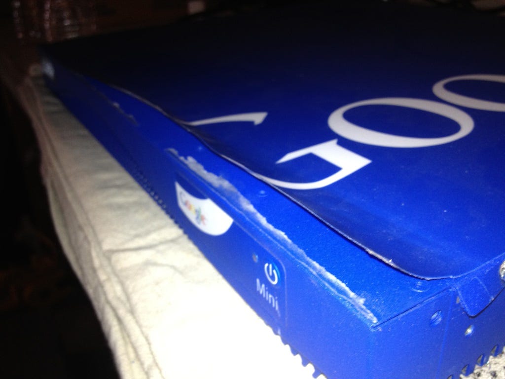
The Google Mini isn’t super special outside from the fact that it’s a 1U server with a big blue sticker on top and the rest of the outside painted blue. There are also a lot of security bits that prevent normal users from opening them up.
The sticker prevents you from opening the lid so we’ll need to peal that back if we want to see what’s inside.
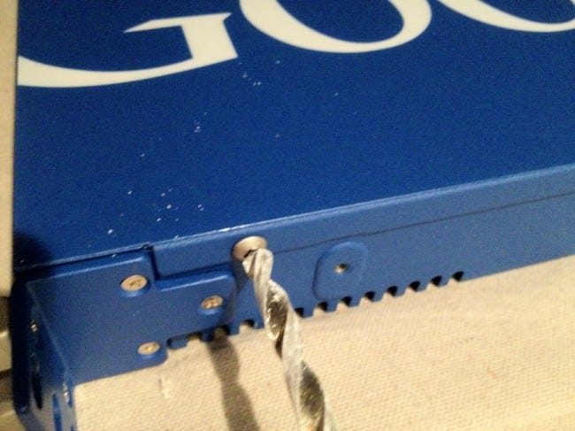
Here’s one of the security screws
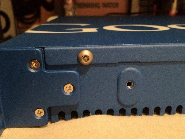
And here’s the master key we’ll use to get inside.
The Internals
Once we get past that we can open up the lid by sliding it back and revealing the insides.
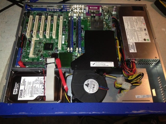
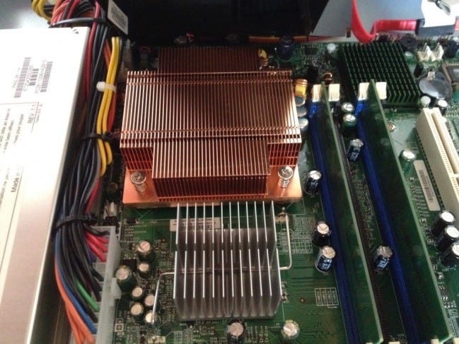
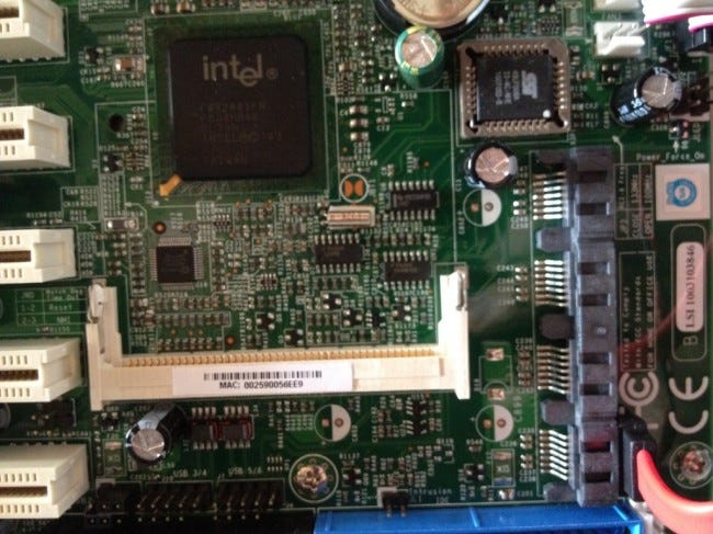
Let’s start by looking at the main components. The CPU heatsink is under the plastic shroud with just a single fan cooling off the entire server. The heatsink below the CPU is for the north bridge which handles communication from the CPU to the RAM. The black heatsink on the top right is for the PCIe controller.
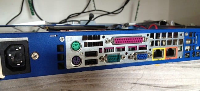
The ports on the server are pretty standard for any desktop/server. An added benefit being this comes with dual network interface cards (NIC) which can allow for more advanced system management.
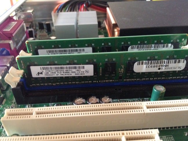
The server comes with 2GB of DDR2 RAM which you can easily see here.
The server has 1 PCIe 16x slot and 5 PCI slots. Not that you could use them in a 1U case though.
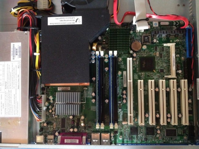
It also has 4 SATA controllers, 1 IDE hard drive controller, and a floppy controller. There is also an IPMI slot which is used for out of band management (OOBM). The slot is missing the OOB network card. You can also see two headers for optional case-mounted USB and some jumpers labelled JWD which stand for Jumper Watch Dog. These jumpers allow the machine to automatically reboot if a software hang is detected.
You can also see the Intel ICH6R south bridge for communication handling to the accessories. The chip near the top right of the picture contains the BIOS and the two pads on the bottom right of the south bridge allow for clearing the CMOS settings when jumped.
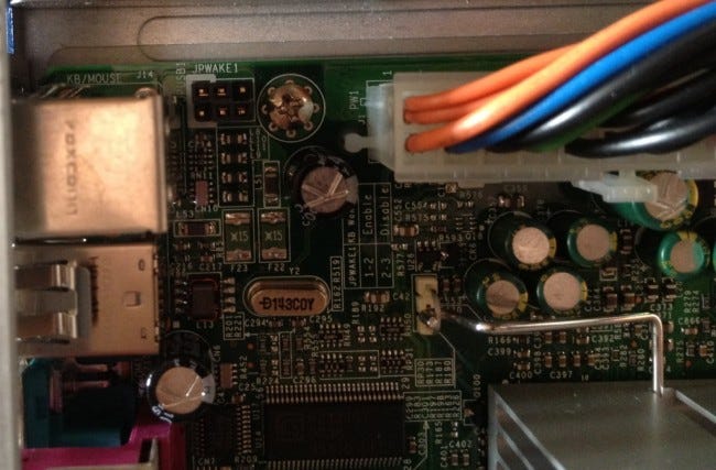
On the other side of the case are some more jumpers. These are labeled JPWAKE1 and JPUSB1. Both of these pins allow the server to be woken either by USB or PS2 keyboard/mouse input.
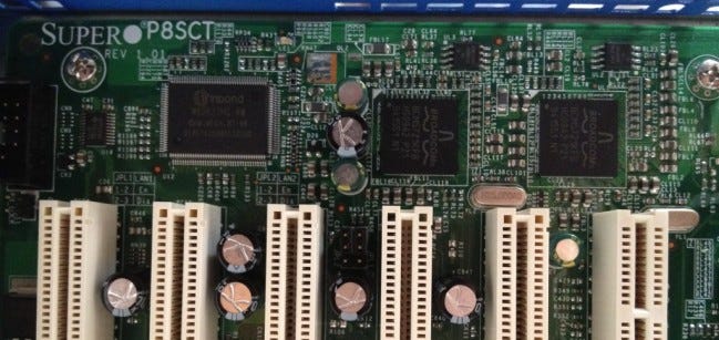
Along the rear of the case are also the two network controllers for the Broadcom network cards. This picture also shows us that the motherboard is manufactured by Supero and the model is a P8SCT. A quick Google search turned up the user manual which proved to be very helpful when identifying some of the chips and jumpers.
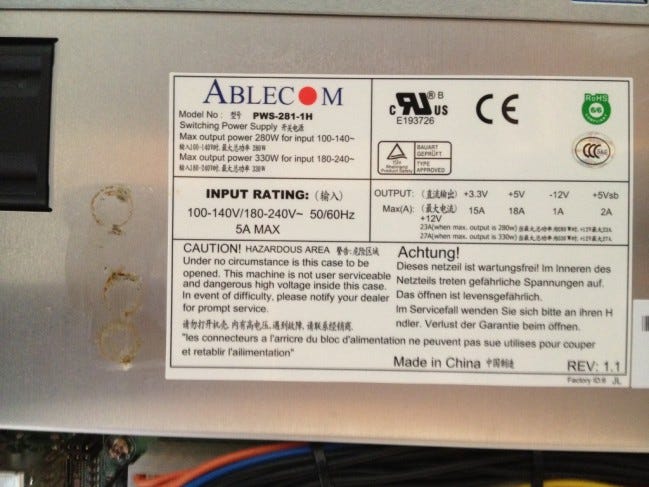
The power supply is standard but to be thorough I might as well take a picture of that too.
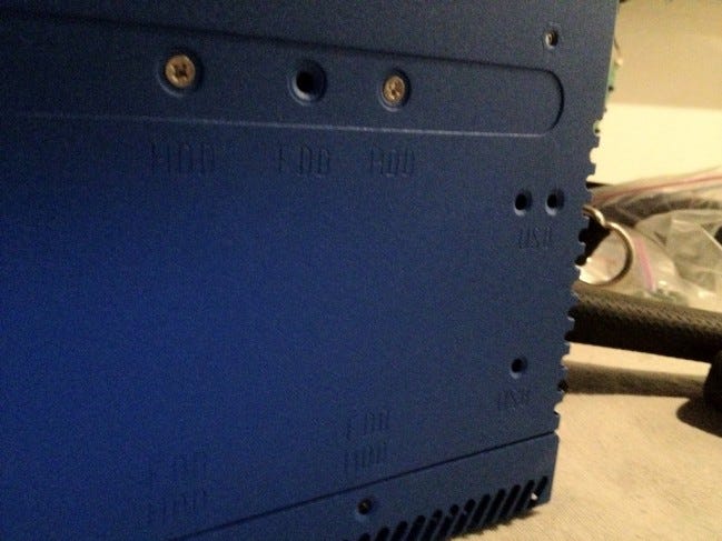
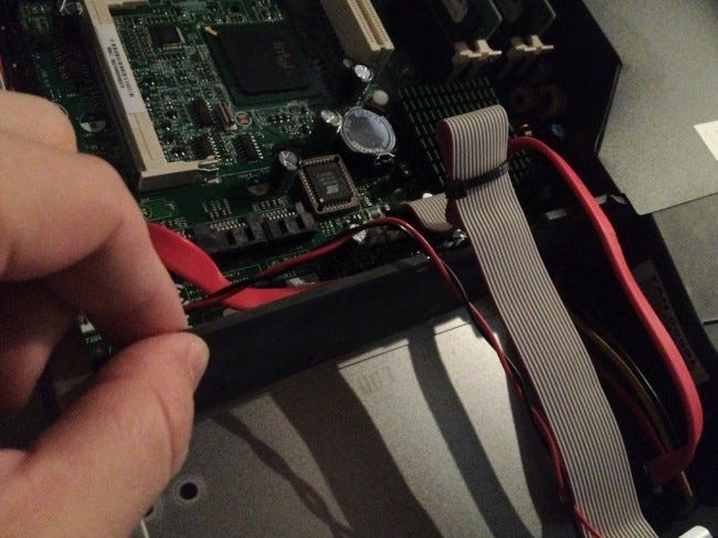
When taking out the hard drive there are 4 screws on the bottom of the case that hold the damper screws to the hard drive. Luckily they’re labeled so it makes finding them easy.
Once you take out the screws the hard drive slides out. There is also a little air dam that keeps air flowing over the hard drive on it’s way to cool the CPU.
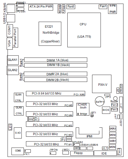
Just to be overly thorough of the motherboard, here’s a component layout from the user manual.
I hope you enjoyed the teardown. Just for comparison, AnandTech their own teardown in 2005 . The internals on that Google Mini looked quite a bit different.
Originally published at 1n73r.net on December 11, 2012.